Advancing the State of the Art for Thin Film Deposition
AI optimized MOCVD and PVD systems enabling next generation 2D materials, semiconductors and other advanced thin film applications
Our Deposition Technologies
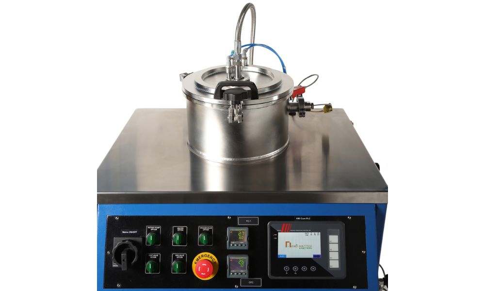
High-throughput epitaxial growth metalorganic chemical vapor deposition systems designed for high-quality 2D material growth with atomic-level control. Supports complex multi-layer film stacks for compound semiconductors, sensors, power electronics, and next-generation photonic devices supporting complex multi-layer film stacks –
- KinetrX AI-powered process optimization
- Precise temperature & flow control
- III-V and II-VI compound capability
- Advanced in-situ monitoring
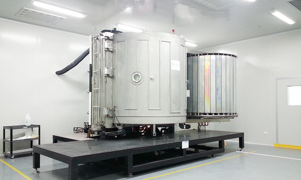
Versatile sputtering and evaporation systems for metals, dielectrics, and complex multi-layer thin film stacks –
- KinetrX AI-powered process optimization
- Magnetron & RF sputtering
- Reactive deposition modes
- In-line and cluster configurations
Deposition as a Service
Partner with NanoMatter to access high-quality MOCVD and PVD processes for your R&D or pilot production. From 2D materials to complex heterostructures, we deliver precision and performance.
Material Expertise
Our team has deep experience with a wide range of semiconductor and 2D materials.
Process Optimization
We work with you to develop and optimize deposition processes for your specific needs.
Analytical Services
Comprehensive characterization and analysis of deposited films and materials.
Success Stories
TIFR Hyderabad Installation
Successfully delivered and installed our advanced MOCVD system at Tata Institute of Fundamental Research, enabling groundbreaking research in 2D semiconductors.
Graphene Innovation
Enabled a research team to achieve record carrier mobility in large-area graphene films using our MOCVD system.
Quantum Dot LEDs
Our PVD system helped develop highly efficient quantum dot LED structures with precise layer control.
Get in Touch
Have questions about our products or services? Our team is ready to help.
info@nanomatter.com
Phone
+1 (555) 123-4567
Headquarters
main road, No. 38/2, 7 th A Cross, Tigalapaya, Peenya 2nd Stage, Balaji Nagara, Bengaluru, Karnataka 560058