Pushing the Frontier of Semiconductors and 2D Materials with atomic-scale controlled deposition
Unlock unparalleled control and scalability with NanoMatter's advanced MOCVD systems for semiconductor wafer sizes up to 8”. Tailored for high-quality epitaxial growth of compound semiconductors and cutting-edge 2D materials our systems enable robust industrial production while also supporting flexible research.
What is MOCVD?
Metal-Organic Chemical Vapor Deposition (MOCVD) is a state-of-the-art thin-film deposition technique that enables atomic-level control of compound semiconductor and 2D material growth. By precisely delivering metal-organic precursor gases into a heated reactor, MOCVD deposits uniform, high-purity epitaxial layers with nanometer precision.
This technology is fundamental to fabricating advanced electronic, photonic, and optoelectronic devices, supporting materials from classic III-V semiconductors like GaN and GaAs to emerging 2D transition metal dichalcogenides such as MoS₂ and WS₂.
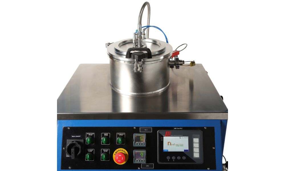
Core Components of a NanoMatter MOCVD System
Reactor Vessel
Engineered for uniform precursor distribution and temperature stability ensuring high-quality film growth.
Gas Delivery System
Precision mass flow control and advanced bubbler technology for repeatable, ultrapure precursor delivery.
Substrate Holder (Susceptor)
High-purity heating platform designed for uniform temperature to avoid defects.
Temperature Control
State-of-the-art heating and feedback loops maintaining exact growth conditions.
Exhaust and Safety Systems
Efficient removal of byproducts while maintaining a clean growth environment.
In-Situ Monitoring Tools
Real-time optical emission spectroscopy and process monitoring for superior reproducibility and control.
Tailored MOCVD Platforms
Research & Development (R&D) MOCVD Systems
Designed for experimental flexibility and material innovation:
- Wide parameter ranges for gases, temperature, and pressure
- Modular, easily configurable reactors
- Compatibility with multiple materials and substrates
- Integrated real-time process monitoring
Industrial Grade MOCVD (Cluster Tools)
Optimized for scalable semiconductor manufacturing:
- Automated multi-chamber platforms with wafer handling and rotation
- Robust precursor delivery for consistent high-throughput
- Advanced process stability for long production cycles
- Large-area uniform epitaxy meeting commercial quality standards
Materials Capability
NanoMatter MOCVD systems grow a broad spectrum of materials including:
III-V Semiconductors
GaN, InP, GaAs
TMDs
MoS₂, WS₂, MoSe₂, WSe₂
Oxides & Nitrides
For optoelectronic and power devices
Emerging Materials
2D electronics and beyond
From next-generation LEDs to 2D electronics, NanoMatter empowers researchers and industrial fabs alike to pioneer breakthrough semiconductor materials and devices.
AI Optimized
Discover settings for maximum performance and reliability
Unscheduled Downtime
AI-driven monitoring minimizes unexpected equipment failures.
Yields
Optimized process parameters improve material and device yield.
Device Performance
Precise control ensures consistent and high-performance devices.
Device Reliability
AI-enhanced stability improves long-term device reliability.
Download NanoMatter MOCVD Datasheet
Explore detailed specifications, configurable reactor designs, and customization options — all crafted to meet your research or manufacturing needs.
Ready to elevate your semiconductor growth capabilities?
Contact NanoMatter today to customize your MOCVD system for research breakthroughs or industrial production excellence.
📧 info@nanomatter.tech
🌐 www.nanomatter.tech